Introduction
Transistors are a fundamental component in digital electronics from which we can build circuits that can perform logic. At their core, they act like on/off switches that can be manipulated electrically, and although this is a simple concept, I had a hard time understanding exactly how they worked in the real world. For example, in a blog post I wrote about understanding a roulette wheel kit, I could not figure what a transistor would be doing as resistor-capacitor series were in the process of charging; how close to being fully charged would the capacitor be before the gate switched on?
A lot of websites explain what NPN transistors accomplish and how the collector, base, and emitter, are related to this behavior. For example, Sparkfun's transistor page breaks down the operating modes of your standard NPN transistor into the following:
- saturation mode happens when the voltage at the base (with respect to ground; Vbase) is higher than both the voltage at the emitter and collector (again, with respect to ground; Vemitter and Vcollector)
- active mode happens when the base voltage (Vbase) is higher than the emitter Vemitter but lower than the collector Vcollector
- cutoff mode happens when the base voltage (Vbase) is lower than both the collector (Vcollector) and emitter (Vemitter)
But just having these relationships and a few equations weren't enough to help me understand how I could use these transistors in actual circuits. So for the sake of developing my own understanding of transistors (specifically, bipolar junction transistors, or BJTs), I set up some tests to characterize the behavior of a 2N2222 NPN transistor.
Building a test circuit
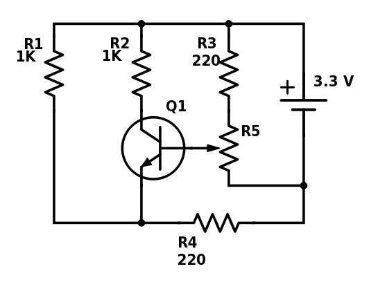
To get a hands-on understanding of what these modes look like in practice, I built a circuit with a 10K potentiometer plugged into the base so that I could see at what point the transistor started conducting:
where
R1pulls up the emitter voltage from ground (along withR4) so that we can demonstrate cutoff modeR2pulls down the collector voltageR3is a backstop to prevent the circuit from shorting when the potentiometer resistance goes to zeroR4pulls up the emitter voltage from groundR5is a 10 KΩ potentiometer to test the effect of changing Vbase on Vemitter
With this circuit, we can directly measure the three voltages that govern the behavior of our NPN transistor by tapping into the circuit at three places:
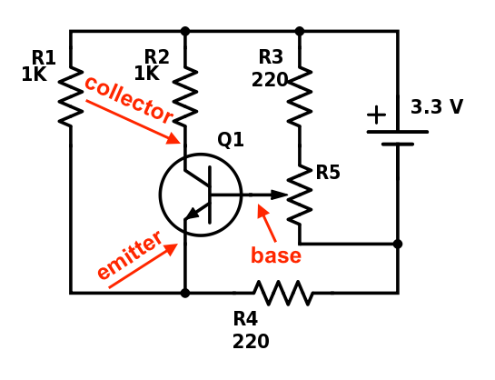
and then taking measurements as the potentiometer is swept from zero resistance to the full 10 KΩ. Using a simple multimeter is the most straightforward way to carry out this experiment, if a bit tedious:

In the above photo, the black clamp is attached to ground, and the red clamp is attached to the collector.
Experimenting with the test circuit
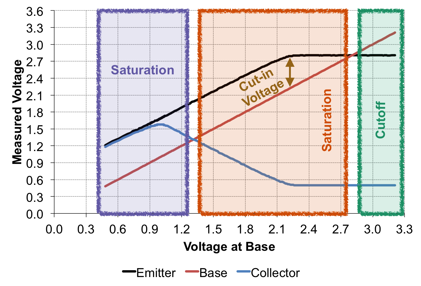
By slowly turning the potentiometer and taking voltage measurements at the collector, base, emitter, we can very clearly see what effect the voltage at the base (Vbase) has on the emitter and collector. Dialing in the potentiometer to set Vbase to values ranging from 0 to 3.3 V in 0.1 V and measuring the other voltages gives us the following:
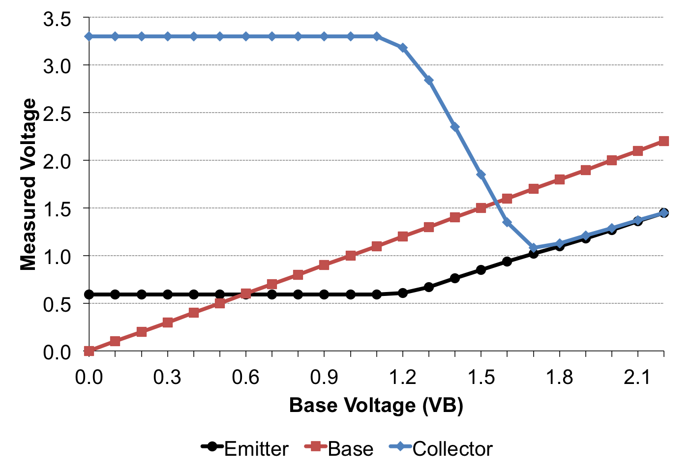
There is a lot of interesting data in this diagram, so let's look at a few things it tells us about NPN transistors.
1. Identifying the different transistor modes
As discussed above, NPN transistors can operate in one of three modes:
| Mode | Criteria | Behavior |
|---|---|---|
| Saturation | Vbase > Vcollector Vbase > Vemitter |
Behaves like closed switch |
| Active | Vcollector > Vbase > Vemitter | Vemitter proportional to Vbase |
| Cutoff | Vbase < Vcollector Vbase < Vemitter |
Behaves like open switch |
On our plot of measured data, these modes are laid out as shown:
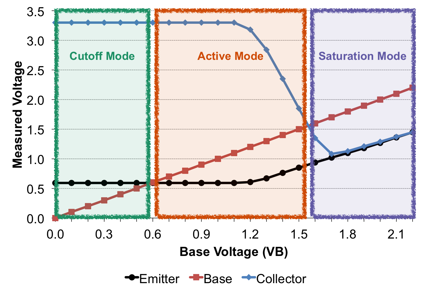
And indeed, we can see that
- in cutoff mode, the collector remains at a constant, high voltage while the emitter remains at a constant low voltage
- in saturation mode, the collector is at the same voltage as the emitter and acts like a short circuit
- in active mode, the collector-emitter voltage difference decreases as the base voltage increases
The behavior in all three regions is remarkably linear; as Vbase is increased, the resulting change in the other two voltages is directly proportional. This is conveniently simple, because other digital componentry (like RC series) do not have simple linear behavior; it is good to know that an NPN transistor does not further complicate that by introducing other nonlinear behavior.
2. Identifying the cut-in voltage
One practical aspect of how transistors work is the voltage range where it should be in active mode, but the transistor is still behaving as if it is in cutoff mode--that is, Vbase > Vemitter but the transistor is still actually not passing any current. In our measured data, this is happening between Vbase values of 0.6 V and 1.2 V:
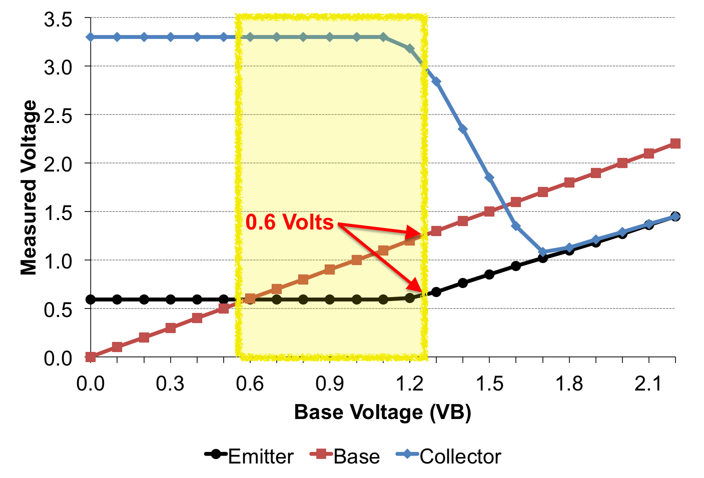
This minimum voltage to get any conductivity is called the cut-in voltage. It turns out that when the difference between Vbase and Vemitter is below this 0.6 V cut-in voltage, the transistor behaves as if it was still in cutoff mode. This VBE < 0.6 V criteria is an intrinsic property of the transistor; even if Vcollector is 5 V (or higher), this threshold of 0.6 V remains constant.
This is a critical property of bipolar junction transistors since any source of resistance you put after the emitter will pull up Vemitter and therefore increase the Vbase you need to supply in order for the transistor to start conducting. For example, attaching an LED to the emitter in a 3.3 V circuit might not always work as desired--you've only got 0.7 V to play with ahead of the collector after the 2.0 V drop from the LED and this 0.6 V cut-in voltage.
Characterizing PNP transistors
PNP transistors can operate in one of three modes:
| Mode | Criteria | Behavior |
|---|---|---|
| Saturation | Vbase < Vcollector Vbase < Vemitter |
Behaves like closed switch |
| Active | Vemitter > Vbase > Vcollector | Vemitter proportional to Vbase |
| Cutoff | Vbase > Vcollector Vbase > Vemitter |
Behaves like open switch |
which, when compared to the table for NPN transistors, represents almost the entire opposite of NPN modes. And if we plug a PNP resistor (like a 2N2907) into our test circuit as-is and run the experiment, we get very strange results:
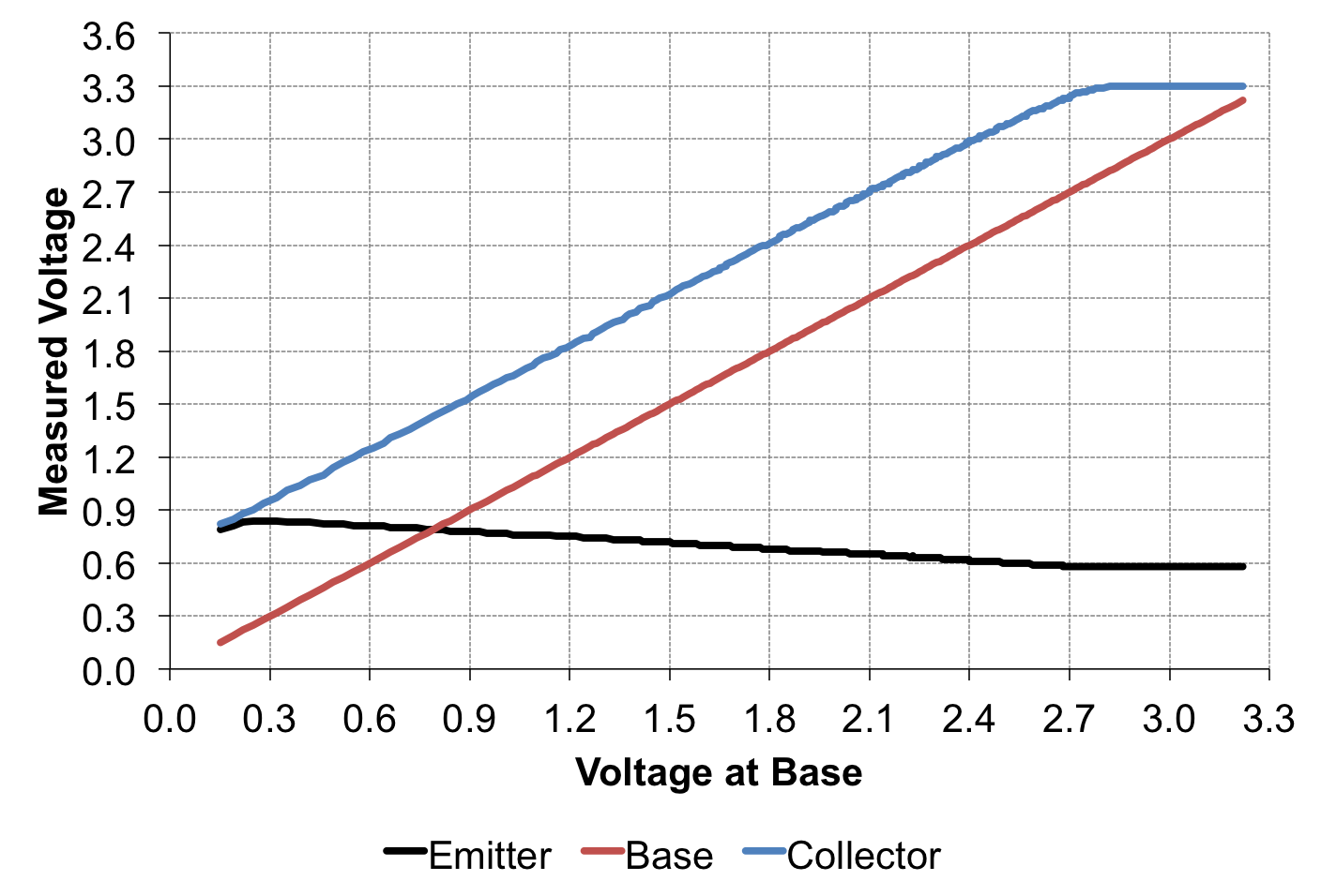
According to the above table, just about all values of Vbase we tested is occurring in a fourth mode which is called reverse-active mode, where Vemitter < Vbase < Vcollector. This happens because the current flows from the emitter to the collector in PNP transistors; we've just run our PNP transistor backwards!
To apply the experimentation technique that we used to characterize NPN transistors on PNP transistors, there there are a few changes we should make to our test circuit:
- We have to replace the NPN 2N2222 with a PNP 2N2907 and reverse the polarity so that the emitter is at a higher voltage than the collector.
R1should be connected afterR2now. In our NPN test circuit,R1's job was to pull up the voltage on the low side of the transistor so that we could observe cutoff mode where Vbase was lower than Vemitter. In this PNP test circuit, cutoff mode will be observed when Vbase is higher than Vemitter, so movingR1will pull down Vemitter from our +3.3 V source.R2should be replaced with a lower resistance so that we can observe saturation mode. In the NPN test circuit,R2's job was to pull Vcollector down below Vbase, where Vbase was governed (in part) byR3. Saturation mode in this PNP case requires that Vemitter be higher than Vbase (again, governed in part byR3), soR2should not be larger thanR3.
Applying these three changes results in a circuit that looks like this:
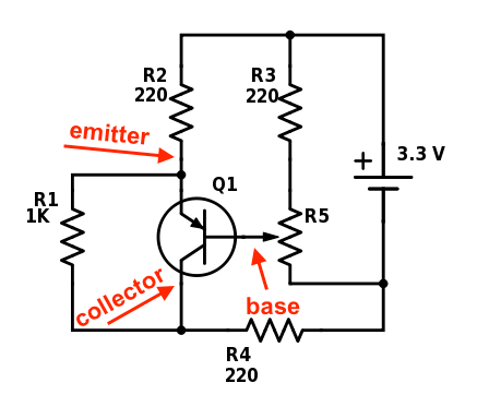
Note that because the emitter and collector are physically reversed, we must take care not to forget which transistor lead we are measuring with our multimeter!
This PNP transistor test circuit demonstrates the following relationships between Vcollector, Vbase, and Vemitter:
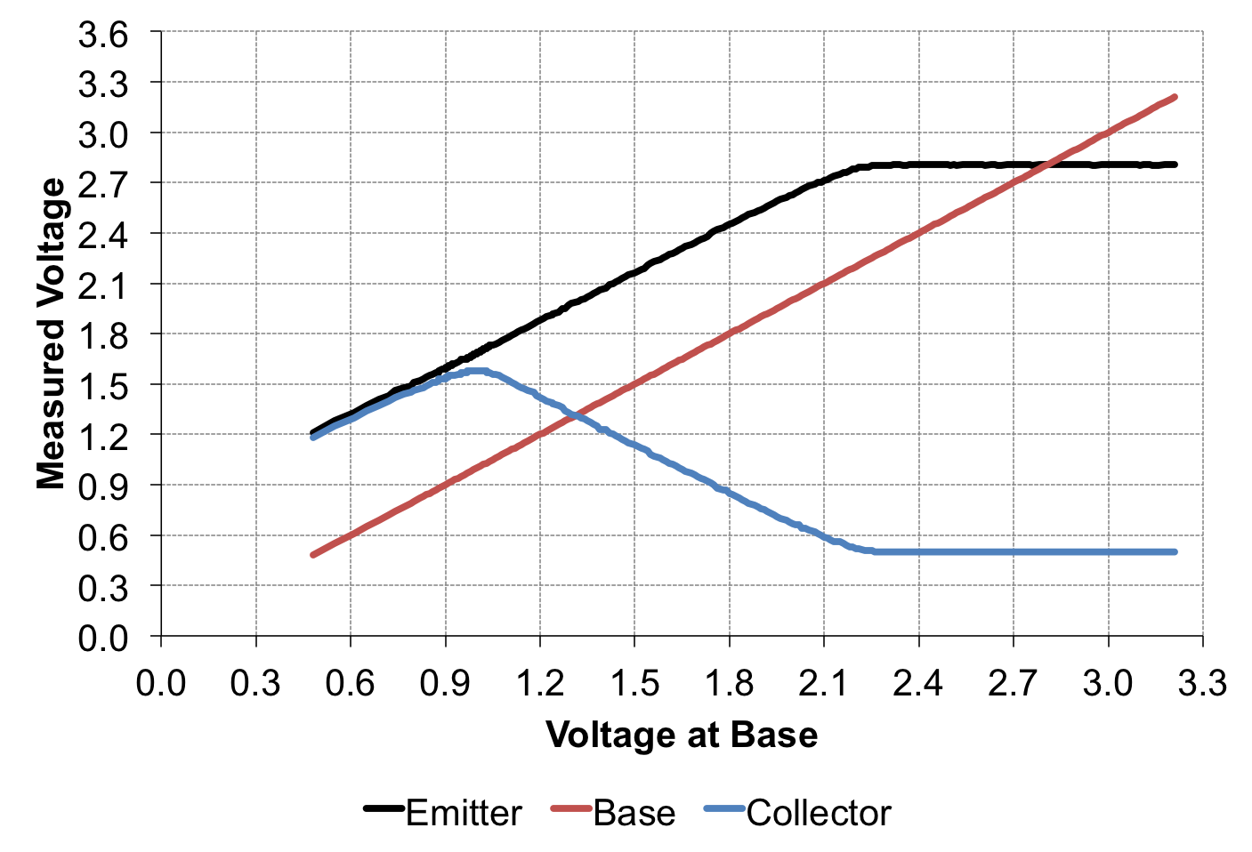
At a glance, this may look quite different from the NPN transistor voltage plot from the previous section. However, if you look at it upside down, you may be able to see how similar PNP and NPN transistors are. All of the same modes are present, as is the cut-in voltage:
The only difference, as any textbook will tell you, is that PNP transistors are "on" when the base voltage is low.
Next steps
These experiments are elucidating, but they are also very tedious to carry out with a mechanical potentiometer and a handheld multimeter. To perform this sort of characterization on more elaborate circuits such as logic gates, we need a more efficient way of varying voltage and taking measurements. To this end, I've written on a page on how to use a digital potentiometer (digipot) and an analog-digital converter (ADC) along with Raspberry Pi to automate these experiments.